Semiconductors are the foundation of modern technology, ensuring the smooth operation of electronics ranging from your mobile phone in your pocket all the way to the cutting-edge medical equipment that saves lives every day. Advancements in electric vehicles, edge computing, and the growth of AI technology are driving the semiconductor market every day. Fabricating semiconductors involves incredibly precise processes, steps like photolithography, deposition, etching, ion implantation and diffusion, are all performed in ultra clean contaminate-free environments. This makes high purity gas and fluid handling systems not just important, but absolutely fundamental to ensuring high manufacturing yields.
Overview of Semiconductor Manufacturing
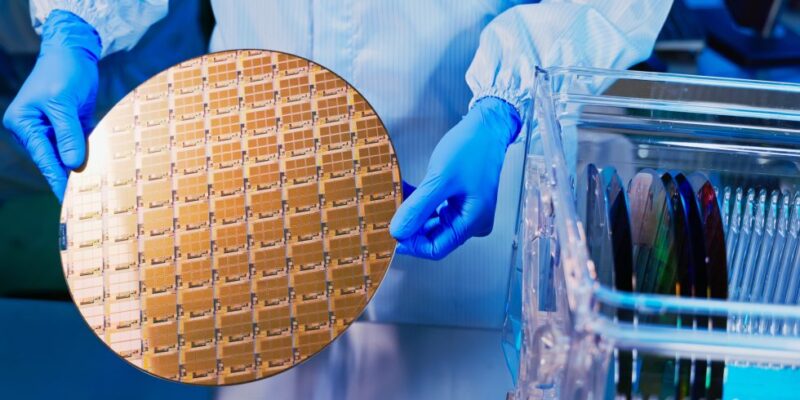
The manufacturing of semiconductors involves several critical stages, each playing a vital role in the development of the devices. It begins with Wafer Preparation, where silicon is refined and reshaped into ingots before being sliced into discs known as wafers. This stage is followed by a series of process steps; deposition, photolithography and etching, where a light sensitive photoresist is applied to the wafer. Unprotected areas of the wafer are etched away, creating nanoscopic structures essential for the circuit’s functionality. Stages of Ion Implantation and diffusion dope the material, where ions are introduced to areas of the wafer, altering its electrical properties to form functional semiconductor material.
Wafer Preparation
As discussed above, the first stage of semiconductor manufacturing is Wafer Preparation. This begins with the formation of silicon ingots using the Czochralski method, where high-purity silicon is melted and cooled into a single crystal. This crystal is then sliced into thin wafers, which are then polished to achieve a smooth, uniform surface. This stage is crucial for preventing imperfections, contamination, or defects which might impact overall semiconductor functionality
Deposition, Photolithography and Etching
The deposition process involves adding ultra-thin layers of metals or insulating compounds to the surface of the wafer. After deposition, the photolithography process is where a photoresist layer is added to the wafer using a spin coating method, ensuring an even thickness of application. Depending on the intended purpose of the process step, either a positive or a negative photoresist is used. The wafer is then exposed to UV light; this process transfers the complex circuit patterns onto the surface of the wafer. After this, the etching process removes specified areas of the wafer, forming the detailed structures required for the integrated circuit. Together, the deposition, photolithography and etching processes create the precise and complex patterns essential for the semiconductor’s functionality. The production cycle can contain many, many cycles of the process.
Ion Implantation and Diffusion
During the Ion Implantation process, charged ions are accelerated and carefully directed onto the wafer’s surface to introduce controlled impurities (doping). These impurities enable conduction, thus facilitating the operation of the semiconductor, creating n-type or p-type material. The Diffusion process involves creating doped regions by exposing the wafer to high temperatures in a furnace. Heating the wafer allows the dopants to penetrate deeper and spread into the silicon. This process also supports the functionality of the semiconductor.
High Purity Welding in Semiconductor Manufacturing
High purity welding is vital within the semiconductor manufacturing process, where purity and precision are essential to ensure a functioning chip. Orbital Fabrications is a trusted supplier of high purity gas and fluid handling systems for a range of semiconductor manufacturers, ensuring a contaminate-free semiconductor. Backed by CHAS Elite accreditations, our team delivers flawless, leak-free welds, providing integrity within the gas and fluid handling pipework which in turn delivers the gases used throughout the semiconductor manufacturing process. From the cylinder to the point of use process.
Importance of High Purity Welding
As highlighted above, semiconductor manufacturing demands exceptionally clean, fully penetrated welds to prevent leaks throughout the system. Without this level of precision, the gases themselves are at risk of becoming compromised by contaminants such as moisture, particulates, or other impurities, which would undermine the manufacturing process. Even the smallest leak can disrupt the functionality of the entire semiconductor, underscoring the importance of flawless welds. Leak integrity is also vital as the process gases used throughout are extremely hazardous.
Applications in Semiconductor Manufacturing
High purity welding is integral to constructing the stainless steel process pipework needed, ensuring the safe and efficient transportation of gases around the manufacturing facility for semiconductor production. Orbital Fabrications is an industry leader in designing, manufacturing, and installing high purity gas and fluid handling systems. Our experienced team works with 316 stainless steel, as well as high nickel content alloys, meeting the rigorous specifications of the semiconductor sector. We also provide complete on-site installations, including comprehensive mounting and support infrastructure solutions where necessary.
Quality Control and Improvement
In semiconductor manufacturing, the gases conveyed through the high purity pipework systems are integral to the process, but also can pose hazards such as being corrosive, pyrophoric, toxic, and flammable. To prevent leaks, high purity welding is essential. Orbital Fabrications utilises the TIG GTAW process to achieve fully penetrated, repeatable, and controlled welds. These welds are resistant to vibration, ambient thermal fluctuations, and are leak-free. Additionally, Orbital Fabrications offers an NDT weld validation service to ensure that your system is completely leak-free and operational.
Quality Control Techniques
As part of our on-site installation service, Orbital Fabrications is able to perform a qualification weld at the start of every on-site shift, or when a material is changed, providing reassurance of our unmatched quality. After the installation of your high purity gas and fluid system, we perform a complete full system leak test using a helium mass spectrometer, offering exceptional sensitivity down to ppm levels of leak detection. To further validate your system, we also complete a pressure test to beyond the normal operational limits. With years of experience in the semiconductor sector, we also supply all required documentation to validate your system, including certificates of conformity, radiography certification, 3.1 material certification, and comprehensive weld maps and logs.
Performance Improvement Strategies
In pursuit of Moore’s Law, which predicts the doubling of transistors on integrated circuits every two years, semiconductor technology has seen rapid development and advancement. Modern chips now offer significantly improved processing power, and increased energy efficiency. These advancements make it essential for all semiconductor manufacturing equipment to be of the highest quality. By providing industry leading high purity gas and fluid handling systems, Orbital Fabrications can help with advancements in the semiconductor manufacturing industry.
Conclusion
The semiconductor manufacturing process is complex, and requires the highest levels of precision, reliability, and purity to ensure that every chip functions as expected. High purity welding plays a crucial role in ensuring smooth operation across the various stages of semiconductor manufacturing, from wafer preparation through to photolithography and etching, and ion implantation.